Materials with strong correlations between charge, spin, orbital, topological and lattice degrees of freedom can exhibit exotic quantum phenomena that has inspired a new generation of devices for computing, communication, energy harvesting or sensing. As for any other material in the past, their successful technological application depends on two factors: a fundamental understanding of the emerging phenomena, and the capability to engineer and tune their key properties. Our group faces this two-fold challenge by exposing electrons to superlattice potentials created by surface atomic steps. A fundamental insight of the interaction of electrons with the step potentials is also obtained by studying electron scattering at individual steps by STM.
Scattering of spin-degenerated electrons in single and coupled step resonators
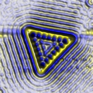
At the nanoscale electron scattering leads to well-known quantum effects such as quasiparticle interference and electron confinement. These were elegantly demonstrated with real-space visualization in the pioneering scanning tunnelling spectroscopy experiments using quantum resonators on metallic surfaces. Here, resonators of different geometry and chemical nature were artificially fabricated by moving atoms one by one, and later used as quantum laboratories for quantitative studies of scattering parameters, and for the exploration of more exotic phenomena such as the quantum mirage and invisibility.
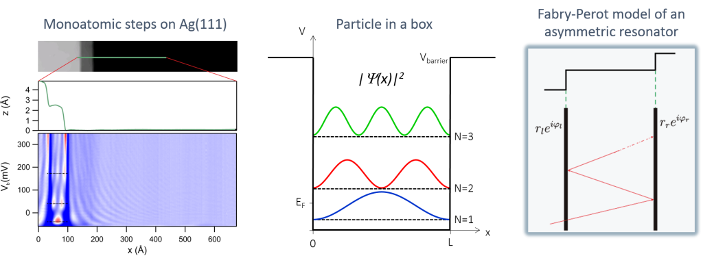
In our approach we use monoatomic steps that are present on the surfaces as natural scatterers to confine electrons. This allows us to go from single to couple resonators by creating self-assembled step superlattices.
Scattering phenomena can be studied with atomic spatial resolution in isolated resonators consisting on parallel pair of steps. Here multiple scattering gives rise to resonances that can be analysed within a Fabry-Perot model in order to obtain the reflection and transmission coefficients and the corresponding phases.

On the other hand, coupled arrays of resonators can be studied using naturally assembled step superlattices that are formed on selected surface orientations that are close to high symmetry directions, such as the (111). This allows the study of electron confinement and propagation by using spatially averaging techniques such as ARPES. Curved crystals are particularly suited for ARPES studies, since they enable a continuous variations of the vicinal angle, and correspondingly of the step superlattice periodicity as we move along the curvature. Our group has been studying the scattering of spin degenerated surface states in such step resonators, observing effects such as superlattice band folding and minibandgap opening [J. Phys. Condens. Matter 18, S27 (2006)], or the electronic stabilization of superlattices by Fermi nesting [New J. Phys. 20, 073010 (2018)]. These studies, in combination with those carried out in isolated resonators by STM provides a comprehensive insight into the fundamental mechanisms that govern scattering.

Related publications:
- “Electron Confinement in Surface States on a Stepped Gold Surface Revealed by Angle-Resolved Photoemission” Phys. Rev. Lett. 87, 107601 (2001).
- “Modelling nanostructures with vicinal surfaces” J. Phys. Condens. Matter 18, S27 (2006).
- “Scattering of surface electrons by isolated steps versus periodic step arrays” Phys. Rev. B 87, 115425 (2013).
- “Metallic thin films on stepped surfaces: lateral scattering of quantum well states” New J. Phys. 16, 123025 (2014).
- “Structure and electronic states of vicinal Ag(111) surfaces with densely kinked steps” New J. Phys. 20, 073010 (2018).
- “Electronic States of Vicinal Surfaces” in Springer Handbook of Surface Science (eds. Rocca, M., Rahman, T. S. & Vattuone, L.) 351–385 (Springer International Publishing, 2020).
Spin-Dependent electron scattering at graphene edges
The electronic structure at the interface between graphene and metal contacts determines the charge and spin injection efficiency into graphene and is therefore a fundamental issue for the performance of nanodevices. The graphene-Ni interface represents an interesting case where the strong interaction with the ferromagnetic substrate opens hybridization gaps and induces magnetic moments. Consequently, graphene is predicted to behave as a perfect spin filter in contact with a magnetic Ni electrode.
Motivated by the interesting spin filtering effect in vertical Graphene/Ni heterostructures, we studied the lateral scattering of the spin split Ni(111) surface states at the edges of graphene nanoislands [Phys. Rev. Lett. 112, 066802 (2014)]. We find a similarly effective spin filtering effect, although the mechanism behind is very different from the spin filtering of bulk electronic states in vertical heterostructures. In the latter, the minority states are transmitted more effectively due to a spin-dependent energy matching with the spin polarized graphene bands induced by the interaction with Ni. Conversely, in the lateral direction, it is the perturbation of Ni(111) surface states by the strong interaction with graphene which plays the major role. The surface states under graphene nanoislands are upshifted, resulting in an energy mismatch that effectively quenches transmission. This, however, only occurs for majority states, since the close proximity to bulk states in reciprocal state allows minority states to couple to bulk states that effectively transmit under the graphene nanoisland. The scattering amplitude of majority states depend on the atomic structure of graphene edges, as well as on the electron energy and orbital character.

Related publications:
- “Spin-Dependent Electron Scattering at Graphene Edges on Ni(111)” Phys. Rev. Lett. 112, 066802 (2014).
- “Substrate-Induced Stabilization and Reconstruction of Zigzag Edges in Graphene Nanoislands on Ni(111)” J. Phys. Chem. C 119, 4072–4078 (2015).
Scattering of electrons with strong spin-orbit interaction
In materials with strong spin-orbit interaction (SOI) electronic states are characterized by a particular spin texture that is locked to the momentum, which gives rise to novel magnetoelectronic and transport properties that can be used to manipulate spins. This phenomenon is known as the Rashba effect when it occurs in 2D electron gases at metallic and semiconducting surfaces and interfaces as a result of the broken inversion symmetry. Since its prediction several decades ago, the search for methods for enhancing the Rashba splitting has been unceasing, with a record Rashba parameter of aR=3.05 eVÅ (1-2 orders of magnitude larger than in noble metals) that was recently obtained by adding submonolayer amounts of a heavy element (Bi) to the surface of a light element metal (Ag) to form the so-called BiAg2 Rashba alloy.
In our group we have used the 2D electron gas of this single layer Rashba alloy to study the role of SOI on the scattering. The scatterers of choice are again isolated and coupled resonators created by monoatomic steps, studied by STM and ARPES correspondingly, following a similar methodology as that carried out with spin degenerated electrons (see Scattering of spin-degenerated electrons in single and coupled step resonators ).

An important finding in our study derives from the analysis of QPIs formed by scattering at single steps [Phys. Rev. Lett. 114, 166801 (2015)]. The scattering events related to the QPI pattern couple states of opposite spin, a forbidden event in single orbital bands when time-reversal is conserved, as it is the case in a Rashba system. The scattering channel experimentally observed is possible due to the orbital degeneracy of the band, that allows a combined orbital and spin transition that conserves the total momentum. This new spin-flip mechanism is very effective in steps with a high density of Bi atoms, where the orbital/spin flip is aided by a significant SOI, but results in weak interferences in other step directions where the presence of Bi is more diluted. We also show that the respective localization of occupied and unoccupied bands on the Ag and Bi planes of the BiAg2 bilayer leads to shifted element-specific potential barriers for steps consisting of alternate Bi and Ag rows (A-steps).


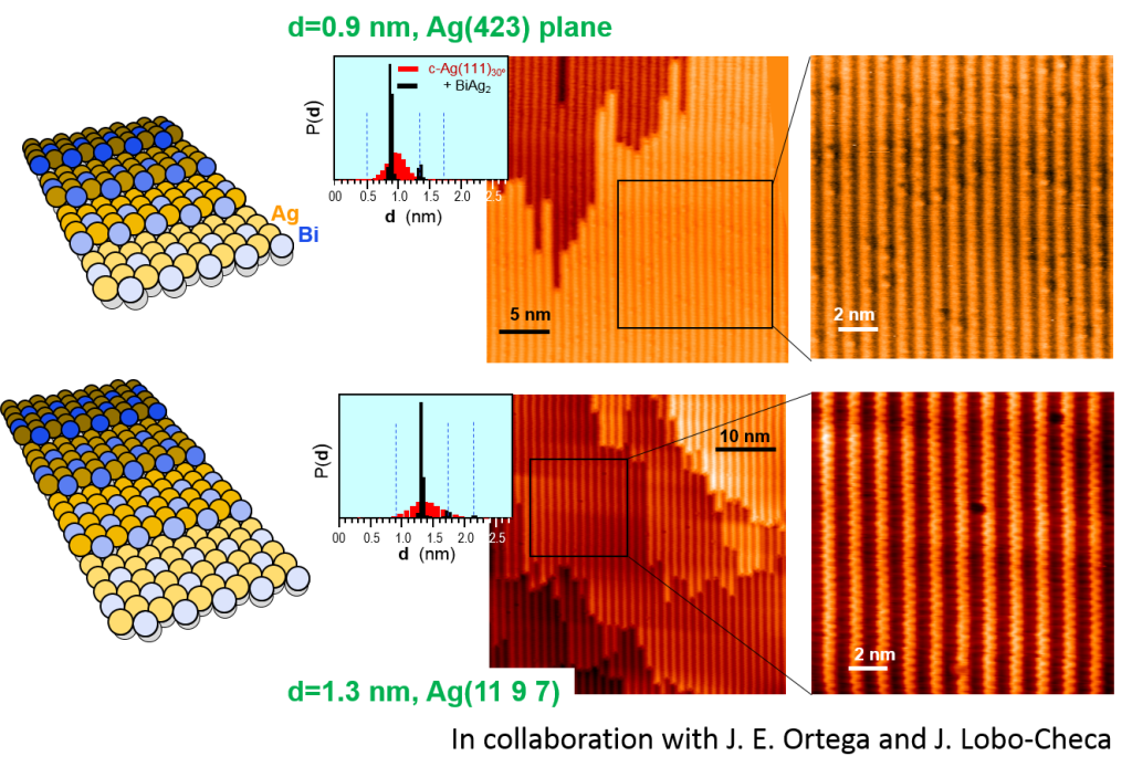
For the ARPES study we fabricated BiAg2 superlattices on a curved Ag(111) substrate [arXiv:1902.05777 (2019)]. We find that, by choosing the right atomic structure of the steps by the selection of the azimuthal direction of the curvature, we can obtain atomically precise superlattices for certain magic vicinal angles. This is related to the stabilization provided by the surface alloy unit cell for terrace widths that match integer numbers of its size, similar to that observed in vicinal Si surfaces.


The ARPES measurements carried out in different synchrotron radiation facilities reveal that, for the direction where the strong scattering has been observed in isolated resonators by STM, and where the atomically precise superlattices can be obtained, the effects of the superlattice are pronounced, resulting in strong downshift of Rahsba bands, and clear umklapps or bandfolding. On the other hand, for the direction where the study of isolated resonators resulted in weak resonances, we find marginal effects of the superlattice. The resulting potential barriers derived by a Kronig-Penney model reflect the tunability of potential barriers in this system. The barrier in the strong confinement direction is an order of magnitude larger than that found for the surface states of the parent Ag(111) system. For the weak confinement direction, however, the obtained barrier is smaller than that for Ag(111) surface states. The orbital and spin decomposition of bands carried out by DFT indicate that not only the dispersion of the bands is perturbed by the superlattice, but both the spin and orbital composition are also strongly affected. Altogether, this study shows that the use of step superlattices can be a very effective strategy to engineer the electronic structure, and spin-orbital texture in Rashba systems.

Related Publications:
- “Spin-Flip and Element-Sensitive Electron Scattering in the BiAg2 Surface Alloy” Phys. Rev. Lett. 114, 166801 (2015).
- “Atomically precise step grids for the engineering of helical states”, arXiv:1902.05777 (2019)

