The remarkable electron and heat conductivity, mechanical stiffness, or impermeability has conferred graphene the title of “the wonder material”. Yet, many properties that are relevant for a variety of applications are still missing in this single layer of carbon, namely the semiconducting gap that is essential in (opto)electronics and photonics, the magnetic moments that could be exploited in spintronic devices, or the selective permeability and reactivity that is needed for nanofiltration and sensing applications respectively. This missing properties can be introduced in graphene by means of nanostructuration and functionalization. In our group we employ different bottom-up strategies for the realization of graphene nanoarchitectures where the structure and chemical composition are tailored with atomic precision.

Graphene quantum dots with zig-zag edges
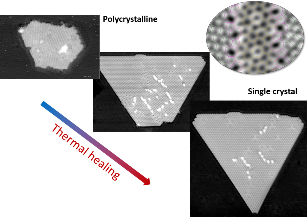
Epitaxial graphene islands grown on close-packed metal surfaces by decomposition of hydrocarbons usually present broad shape and size distributions. By using CVD to grow graphene nanoislands out of propene decomposition on the Ni(111) surface, we have been able to control the yield and shape of the nanoislands. Carefully choosing the reaction/annealing parameters, we can go from irregular clusters to triangles and hexagons larger than 100 nm2 and with well-defined edges [Nano Lett. 12, 4431 (2012)].

By high resolution STM imaging, we have been able to resolve the orientation of the different domains and the atomic structure of their boundaries, as well as the stacking of each to the underlying Ni(111) [2D Mater. 4, 025104 (2017)]. In this study we found a non-conventional multistep mechanism that separates the thermal regimes for growth, edge reconstruction, and final stacking configuration, leading to nanoisland morphologies that are incompatible with their stacking symmetry. A statistical analysis of the domain structures obtained at different annealing temperatures reveals how polycrystalline, ill-defined structures heal into shape-selected islands of a single predominant stacking. The high crystallinity and the control on morphology and edge structure makes these graphene nanoislands ideal for their application in optoelectronics and spintronics.

Related publications:
- “Yield and Shape Selection of Graphene Nanoislands Grown on Ni(111).” Nano Lett. 12, 4431 (2012).
- “Substrate-Induced Stabilization and Reconstruction of Zigzag Edges in Graphene Nanoislands on Ni(111).” Phys. Chem. C 119, 4072–4078 (2015).
- “Symmetry forbidden morphologies and domain boundaries in nanoscale graphene islands.” 2D Mater. 4, 025104 (2017).
- “Spin-Dependent Electron Scattering at Graphene Edges on Ni(111).” Rev. Lett. 112, 066802 (2014).
Stabilizing edge functionalization of graphene nanoribbons
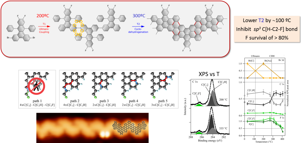
Bottom-up nanoarchitectonics has demon-strated the capability to control structural parameters of nanomaterials with atomic precision. The surface-assisted synthesis of graphene-based one-dimensional nanostructures à la carte distinctly illustrates the power of this concept. However, despite impressive advances in the synthesis of 1D homostructures, introducing heteroatoms and functional groups is often challenged by their stability during the reaction path of the on-surface synthesis. The functionalization of edges in nanoribbons, an effective strategy to tailor their electronic properties and chemical interactions, is particularly affected by this issue due to the weaker bonds of functional groups as compared to substitutional heteroatom dopants.
The main burden that affects the stability of functional groups are the weakening of the linking bonds by interaction with side products. Indeed, it has been shown that hydrogenation of the functionalized carbon atom can lead to the total defluorination, despite the C-F being one of the strongest bonds in chemistry [ACS Nano 11, 6204–6210 (2017)]. In our group we have overcome this issue by designing precursors that do not jeopardize the stability of the functional groups by unwanted interactions of the functionalized site with the residual hydrogen that comes from the cyclodehydrogenation step. This strategy, together with a reduction of the final reaction step by 100ºC, led to the survival of 80% of the fluorine groups in the synthesis of GNRs [ACS Nano 14, 11120–11129 (2020)]. A similar strategy was followed in collaboration with J. I. Pascual at Nanogune, where amine functionalized chiral GNRs were achieved with a survival of 75% of the amine groups [ACS Nano 14, 1895–1901 (2020)]. Interestingly the two functional groups lead to opposite band shifts of the corresponding GNR, representing realizable examples of n- and p-doping.

Related publications:
- “Edge Fluorination in Graphene Nanoribbons” ACS Nano 14, 11120–11129 (2020).
- “Band Depopulation of Graphene Nanoribbons Induced by Chemical Gating with Amino Groups” ACS Nano 14, 1895–1901 (2020).
From self-assembled GNR superlattices to 2D nanoporous graphene
Despite the impressive advances in the synthesis of graphene nanoribbons, where control on all structural parameters have been demonstrated, the field is far from having similar control on their distribution on the catalytic substrate. This is relevant for i) the long-range order of the individual structures, since the distribution affects their interactions and hence the growth; ii) the realization of suprarribbon (2D) covalent structures, which requires their prior organization; iii) the realization of devices where the GNR orientation needs to be controlled.
One strategy to obtain macroscopic alignment of GNRs in the synthesis is the use of hard templates such as stepped surfaces. This approach, though very effective for the realization of devices with oriented GNRs, limits the length of the individual structures due to the restricted of diffusion in narrow terraces during the growth. More importantly, it impedes the realization of supraribbon structures by the lateral coupling of the individual units.
By using a softer template to guide the synthesis, we have been able to form self-aligned superlattices of GNRs of different periods [Chem. Commun. 54, 9402 (2018)]. The template in this case is the herringbone reconstruction of the Au(111) surface. This provides a zig-zag pattern of tracks of different stacking with the underlying atomic layer separated by domains that protrude few tens of pm due to the local stacking mismatch. Whereas the zig-zag pattern is not suitable for the growth of straight GNRs, the dislocations located at the kinks form a rectangular array that guides the growth of polymers, leading to self-aligned arrays of GNRs. In addition to the formation of superlattices, the alignment facilitates the growth of GNRs, reaching maximum lengths above 100 nm, and average lengths of around 70 nm.

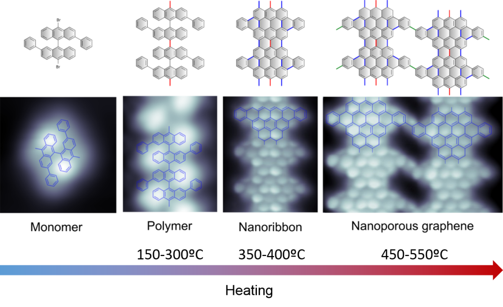
The weak interaction between the GNR and the underlying template allows their lateral diffusion. We have exploited that to induce a new supraribbon reaction that fuses the aligned GNRs [Science 360, 199–203 (2018)]. The resulting structure is a nanoporous graphene (NPG) that combines ~ 1 nm stripes (the backbone of the ribbon), with ~ 1nm nanopores (GNR bridges). Each of these components giving a different functionality: the electron confinement along the GNR stripes makes the nanomaterial a 1-2 eV semiconductor, and the weak interribbon coupling makes it strongly anisotropic. On the other hand, the nanopores can enable selective permeability and filtering of small molecules and ions. The coexistence of both functionalities makes this nanoporous graphene a highly versatile semiconductor for simultaneous sieving and electrical sensing of molecular species.


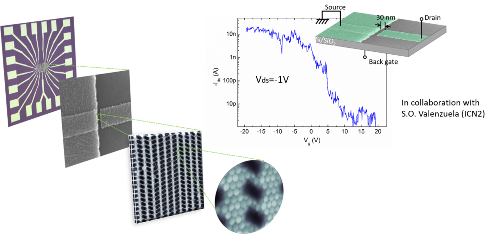
In collaboration with the group of S. O. Valenzuela (PEND group at ICN2), we have been able to fabricate field-effect transistors with the NPG. The NPG-FETs show state of art on-off ratios of 104, though still the on current density of ~ 1 mA/mm orders of magnitude lower than the expected values >20 mA/mm. This can be in part due to the fact that only few of the GNRs of the NPG region within the 100 nm wide electrodes is contacted at both sides, and the well-known problem of Schottky barriers at the interface with contacts (confirmed by the non-linear Id-Vd behavior at low bias). Interestingly, the large scale of our nanostructures as compared to randomly grown GNRs facilitates the fabrication of devices, with a yields of 75% with 30 nm wide channels, as compared to the 10% yield obtained for the maximum channel width of 20 nm for individual GNRs.

Related publications:
- “Bottom-up synthesis of multifunctional nanoporous graphene” Science 360, 199–203 (2018).
- “On-surface synthesis of superlattice arrays of ultra-long graphene nanoribbons” Commun. 54, 9402 (2018).
- “Critical Role of Phenyl Substitution and Catalytic Substrate in the Surface-Assisted Polymerization of Dibromobianthracene Derivatives” Mater. 31, 331 (2019).
- “Nanoarquitecturas de grafeno con precisión atómica” Española Física 33, 1–6 (2019).
Beyond nanoporous graphene: lateral heterostructures
The realization of GNR superlattices can be exploited to go one step beyond and depart from homogeneous to heterogeneous NPGs. This can be done by introducing additional steps in the method developed to synthesize NPG. Once we create the superlattice of decoupled GNRs, we introduce a new precursor that can lead to the synthesis of a new GNR component intercalated within the initial GNR array. The mixed array can now be fused into a heterogeneous NPG by the lateral fusion of the GNR components. We have demonstrated this strategy by creating a heterogeneous NPG that contains undoped and N-doped 7-13-AGNRs as intercalated components [Adv. Mater. 34, 2110099 (2022)]. Seen by structural googles, we can define the new structure as nanoporous graphene with selective, atomically precise doped pore edges. On the other hand, our electronic googles reveal a lateral superlattice heterostructure formed by the intercalated GNRs. The particular electronic properties of the heterocomponents and the interface structure results in atomically sharp band discontinuities that host subnanometer quantum dipoles, altogether enabling the realization of 1 nm scale superlattice heterojunctions.
The sharp band discontinuity together with the presence of tun- neling states at both sides of the junction is expected to pro- mote interribbon excitons, the 1D analogue of interlayer excitons in vertical heterostructures, as well as efficient charge separation that can be relevant for optoelectronics and excitonic solar cells. The coexistence of a type II superlattice band structure with heterogeneous nanopores at the junction makes this graphene-based nanomaterial particularly attrac- tive for photocatalytic applications such as water splitting. Furthermore, the N-doped nanopores of the one atom thick hybrid layer could be relevant for membrane applications such as selective ion sieving.

Related publications:
- “Bottom-up synthesis of multifunctional nanoporous graphene” Science 360, 199–203 (2018).
- “Atomically Sharp Lateral Superlattice Heterojunctions Built‐In Nitrogen‐Doped Nanoporous Graphene” Mater. 34, 2110099 (2022).
